Printed Circuit Boards (PCBs) are a crucial part of any electrical or electronic system. Designing a PCB layout, in a way that delivers the high-speed electrical signals plays a big role in the final output. A PCB not only has to be designed properly with schematics, but it also has to be optimized with algorithms and connectivity and analyzed for limitations. A fully optimized PCB design offers mechanical support to electrical components and makes the device actually work and function for the use it was meant to be.
Needless to say, a PCB is at the heart of any electronic gadget or an electrical device. And to design the PCB in a way that offers high-speed electrical connectivity between electronic components is vital for any product. That is what Integra Sources provides to its clients – a complete solution to PCB design and layout services.
PCB Design and Layout services are at the heart of the immense range of services that Integra Sources offers to its clients. Integra Sources is an electronic design service company, which offers all the essential PCB Design and Layout services for industries. Within its scope, it includes the whole array of services needed and required in a PCB. Following is a snapshot of PCB design solutions by Integra Sources.
Technical Specification

At Integra Sources, the very process of PCB design starts with a Technical Specification. Writing a specification gives a broad overview of what the project will encompass, and what is the feasibility of that project. Specifying the technical details about the project, the mechanical components, tools, and technologies used for implementing the project, the Bill of Materials (BOM), and the BOM costs, block diagrams, and deliverables give a precise idea of the cost estimate of the project. But more importantly, it broadly outlines the entire project in clear detail and gives an idea of its scope to satisfy the demands and expectations of the client.
Recommended for you: Indy Invoice Generator Review: How it Makes Life Easier for Freelancers and Small Businesses?
Schematic Design
A schematic design is a visual representation or a diagram of the PCB before it is actually made. At Integra Sources, PCB designing is done with professional CAD software like the Altium Designer to simplify the PCB design process and eliminate any errors in the PCB design. It visually lays out a design of all the electronic components to be used in the PCB board, the electrical connection between them, and Integrated Circuits (IC) that allows the circuit to flow between components. Along with this, a schematic design also integrates other components with their functions. A schematic design makes the electrical circuit readable and visual.
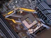
PCB Layout
At Integra Sources, expert engineers manually arrange the electronic components and ICs into the PCB board. Specialists conduct various tests to evaluate the electrical circuit routing of the PCB housing, keeping in mind the limitation of the size of the circuit board. From simpler PCBs to more complex PCB designs, Integra Sources makes layouts and designs in a way that cuts down on the development costs. PCB board design is evaluated, revised, and analyzed with DFM/DFA analysis. The PCB board architecture goes through various simulations to ensure total safety in its working and functions.
PCB Fabrication and Testing

Within the scope of PCB Design and Layout services that Integra Sources provides to its customers, testing on the prototype of the PCB design is very much an integral part of the service. The prototype of the PCB is fabricated after the PCB design layout is approved for production. It is made based on the format that the manufacturer wants. A 3D image is made of the PCB board to make sure it fits the housing. At each stage of developing and fabrication of the PCB, tests are conducted. A Bill of Materials (BOM) is prepared and Gerber files are made to describe the design requirements of each image on the PCB circuit board. Software and data necessary for electrical and impedance testing are provided to manufacturers.
Mass Production

After the prototype is approved, testing the software and hardware is the next service that Integra Sources offers to its clients. Software and hardware are tested in-house. After testing, and prototype validation, files are prepared for mass production of PCBs by the manufacturer. Integra Sources offers technical support and inputs at every stage of the PCB manufacturing process. Procedures on hardware and software are carried out, and data is collected and organized so that clients can test the prototype at their factory.
Technical Support

Giving technical support is an essential part of the services that Integra Sources provides to all its customers. Experts offer valuable help during the PCB development phase as well as after the PCB design and layout are approved and the project is complete. 3D models, BOM and Gerber files, and technical manuals and documents are offered after the project ends. Integra Sources sets a warranty period for the PCB design services. Even after the warranty period ends, they continue to offer services to its customer on the technical aspects of the PCB design and layout.
You may like: Content Writing Services by Topcontent – A Detailed Review.
Delivery Models used by Integra Sources in its PCB Design and Layout Services
Project-based Outsourcing: In Project-based outsourcing, Integra Sources owns complete responsibility for developing the PCB design. From planning to completion, it includes various steps like building 3D models, assembling a prototype, gathering mechanical components and IC circuits, and integrating the same in the PCB design and layout process. By managing the entire project, Integra Sources guarantees complete control over the quality and safety of the PCB board.
Dedicated development team: Integra Sources also aids companies who are looking for an expert and dedicated team of qualified team of hardware engineers to guide their own in-house team in developing the PCB design. Integra Sources also offers companies who need an offshore development team full-time project development cycle in developing the PCB Design and Layout. In collaboration with Integra Sources, companies can shift their focus in controlling the cost of development, and scale their products at their own pace, and be in full control over the project.
Research & development: Integra Sources offers technical and technological know-how in developing the PCB circuit board. It is more beneficial for companies who are not sure about the technological and scientific feasibility of the product and want technical guidance in developing innovative products that are new in the market. Integra Sources can help companies by pointing out the potential risks in the final product, and get a complete understanding of the costs involved in developing the product. Integra Sources offers scientific research involved in developing the PCB design, makes PCB prototypes, and implements the project from start to finish.
Unique things to know about PCB Design and Layout services by Integra Sources
The following questions will bring more clarity to the PCB Design and Layout services offered by Integra Sources:
What technologies does Integra Sources use in making the PCB design and layout?
Integra Sources use the latest electronic design automation software applications like EAGLE, Altium Designer, Cadence Allegro, KiCad, PCad, and OrCad. With the help of these high-precision automation software applications, Integra Sources makes the most demanding and complex PCB circuit designs for industrial uses as well as simpler ones used in consumer electronics and household products like drones, robotic lawnmowers, pet cameras, etc. In-house Engineers at Integra Sources have access to a huge library of components of each of these software applications and make their use for PCB designing. But they can move to more customized solutions, and specific software preferences before actual development begin.
Can Integra Sources design a prototype of the PCB model?
Yes. They makes a prototype of the PCB with all its electronic components. They have all equipment which is required to assemble the PCB prototype and test it before sending it to the manufacturer for mass production.
How many layers do clients get in their PCB board design?
At Integra Sources, Engineers use multiple layers in building the PCB design. The layers in a PCB board can range from anything between 1 to 12.
Is the PCB design validated before production and delivery?
Yes. Validation of the PCB board is a part of the services which Integra Sources provides to its clients. Tests such as Design Use Checks (DRC) are done on the PCB board design to identify and remove errors. Special software is used for building 3D circuit board models of the PCB integrating the schematic block diagrams designed by the in-house team of engineers and technical support staff. Integra Sources also relies on the automation knowledge and technological expertise that they have garnered through the many years that they have in the highly technical field of designing PCB circuit boards.
How can clients know about the price of the final product before it is developed?
Yes. Integra Sources helps its clients get an estimate about the final product before it is even made. Based on the requirements of the client, a list of all the components and technologies, and software is made. A Bill of Materials (BOM) includes all these pre-selected components. If the project needs more customized components, then Integra Sources contacts vendors and manufacturers and makes the necessary arrangements. Engineers can then evaluate how simple or complex the design of the PCB is based on the mechanical components, software, and BOM. Cost is calculated and a rough estimate is then made about the cost of producing PCB boards for devices.
You may also like: Values App Review – A New Way to Discover and Align Your Values.
Final Words

All the above points are enough to point to the fact that developing a PCB Design and Layout is an essential service that Integra Sources provides to its customers and industries. In making simple as well as complex PCB boards, it offers technical and mechanical expertise to its clients and manages the PCB design project from its start to completion.