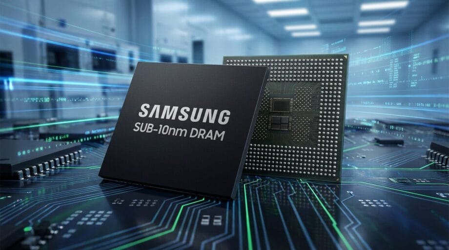
Samsung has achieved a significant milestone by creating the world’s inaugural “standalone” DRAM module utilizing a processing technology that operates below the 10nm threshold.
Samsung’s Innovative Sub-10nm DRAM Technology Promises Enhanced Densities and New Material Utilization
Historically, the DRAM sector has depended on a 10nm process technology for the fabrication of integrated circuits.
Variants within the 10nm scope include 1x, 1y, 1a, 1b, 1c, and 1d iterations. Samsung is now pioneering a novel 10a process technology for DRAM, transcending the conventional “10nm” benchmark.
Samsung Electronics has successfully produced the first operational die of single-digit nanometer DRAM. The company aims to promptly enhance yield by fine-tuning process conditions based on the die’s performance.
As reported by industry insiders on the 24th, Samsung confirmed the working die during the characteristic inspection phase, following wafer production utilizing the 10a process last month.
This progression stems from the inaugural application of the 4F square cell structure combined with the Vertical Channel Transistor (VCT) methodology.
With the 10a process, industry analysts project a scaling down to approximately 9.5-9.7nm, establishing it as the first sub-10nm technology in the market. The advancements facilitating this innovation revolve around the “4F Square Cell Structure” and the VCT process.
Currently, Samsung anticipates finalizing development of the 10a DRAM, with mass production slated for 2028. The 10a structure will undergo iterative enhancements in subsequent generations, 10b and 10c.
The transition to 3D DRAM technology is expected in the 10th generation, projected for release around 2029-2030.
Presently, DRAM offerings employ a 6F architecture, producing rectangular configurations measuring 3Fx2F. The introduction of the 4F design enables a more compact square formation (2Fx2F), thereby increasing cell density within each integrated circuit by 30-50%.
This restructuring not only amplifies capacity but also contributes to energy conservation. The company will only fulfill existing LPDDR4 orders, not future ones.
The forthcoming DRAM will also incorporate advanced materials such as Indium Gallium Zinc Oxide (IGZO), diverging from the silicon materials utilized in previous versions. The use of IGZO mitigates leakage in narrower cells, thereby enhancing data retention capabilities.
In response, competitors such as Micron are postponing their own 4F strategies, opting instead to focus on 3D DRAM developments.
Chinese manufacturers, hindered by restricted access to cutting-edge lithography equipment, may encounter substantial challenges in producing 3D DRAM.
Nevertheless, there exists potential for a design in 3D DRAM akin to that of 3D NAND, which offers a glimmer of hope for these manufacturers.
Concurrently, the advancement of 3D DRAM technology is accelerating, with numerous companies collaborating on solutions to meet the expanding demands within the AI sector.
Source link: Wccftech.com.